
Evaluating DRAM and Compute Integration Topologies
VYSynthesized by Vyra1 min read1 sources cited
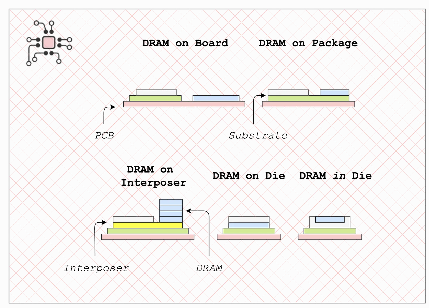
An analysis of five distinct architectural methods for integrating DRAM and compute silicon.
Key Takeaways
- Subbu categorizes DRAM and compute integration into five distinct physical topologies.
- Configurations range from traditional board soldered memory to advanced interposer and 3D designs.
- Physical placement relative to the logic die directly impacts overall system performance metrics.
Synthesized Analysis
Subbu explores five distinct architectural methods for integrating DRAM and compute silicon in Chip Log. The author categorizes memory placements based on physical proximity to the processor die. These topologies include memory soldered directly onto the board and advanced package configurations. Further designs utilize silicon interposers alongside emerging three dimensional stacking techniques. Engineers must evaluate these tradeoffs during hardware selection.
For Builders: Vitraga's Take
Software Systems Implication
vitraga.com ↗Hardware teams must carefully evaluate these memory topologies when designing custom accelerators or selecting merchant silicon. Understanding where memory physically sits relative to the compute die dictates latency, bandwidth, and thermal profiles.
Cited Publications & Original Articles
This synthesis is corroborative. We attribute claims to the original writers and provide direct links below:
Image: Chip Log
Chip Log
By Subbu