
HBM4 Memory Roadmap Brings Massive Bandwidth and Architecture Costs
VYSynthesized by Vyra1 min read1 sources cited
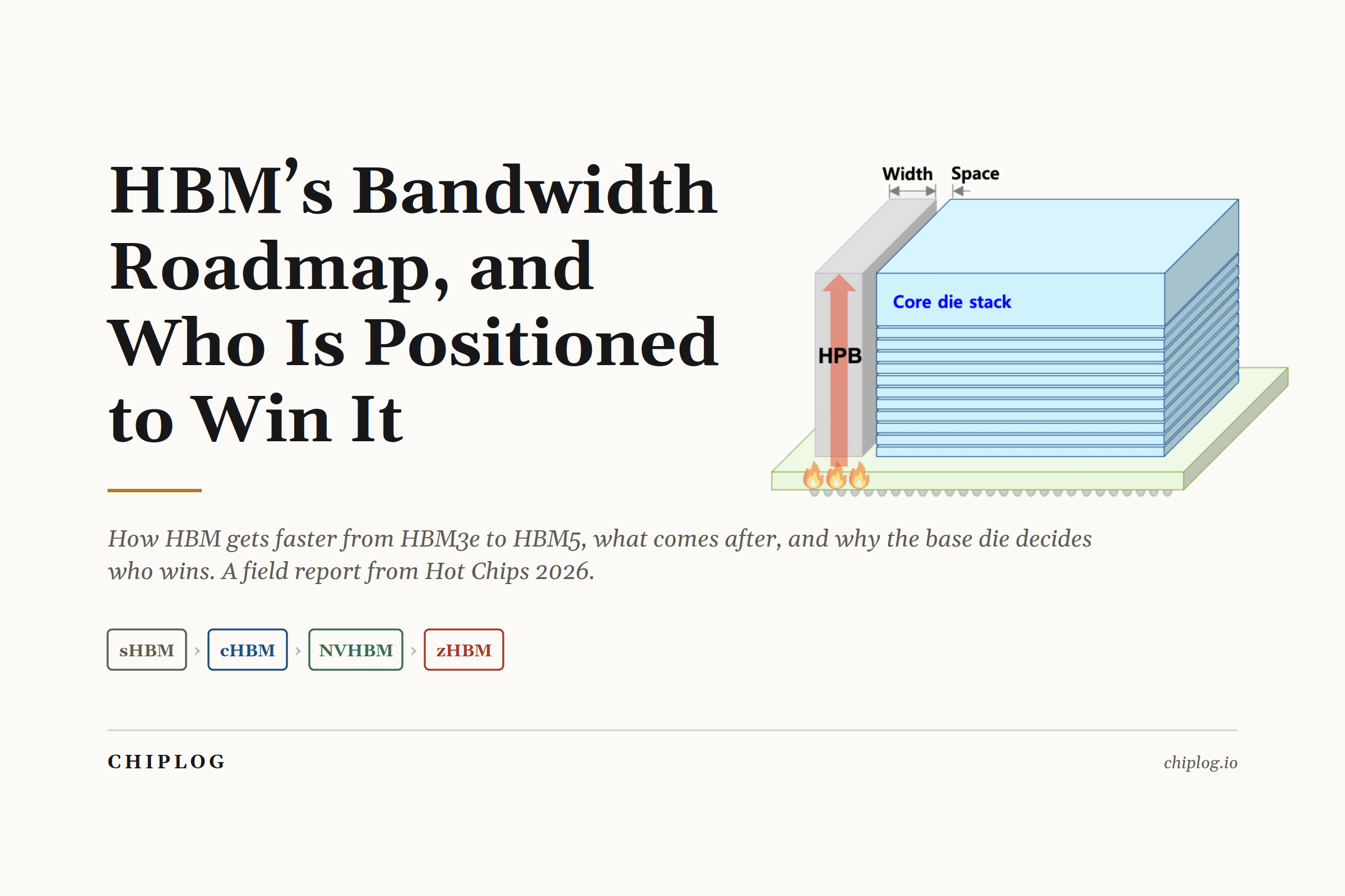
Samsung and SK Hynix outline HBM4 memory advancements while highlighting significant hardware trade-offs.
Key Takeaways
- According to Chip Log, the transition from HBM3e to HBM4 doubles the interface width from 1024 to 2048 bits.
- This hardware evolution allows Rubin systems to support approximately 22 TB/s of aggregate bandwidth.
- The wider interface imposes a significant cost by consuming precious die area on reticle-limited GPUs for larger PHYs.
- HBM base dies also face increased complexity as micro pillar grid arrays and driver circuitry expand to support more I/Os.
Synthesized Analysis
Chip Log author Subbu details how memory manufacturers Samsung and SK Hynix plan to scale aggregate bandwidth up to twenty two terabytes per second for Rubin systems using HBM four technology with a doubled interface width of two thousand forty eight bits instead of the previous standard one thousand twenty four bits which creates serious die area penalties for accelerators.
For Builders: Vitraga's Take
Software Systems Implication
vitraga.com ↗Hardware architects must account for the substantial die area footprint required by larger HBM4 physical interfaces. Software teams should anticipate higher aggregate bandwidth capacities in future accelerator generations, changing optimization strategies for memory-bound workloads.
Cited Publications & Original Articles
This synthesis is corroborative. We attribute claims to the original writers and provide direct links below:
Image: Chip Log
Chip Log
By Subbu