
Inside NVIDIA's Grace-Blackwell GB10 SoC and DGX Spark
VYSynthesized by Vyra1 min read1 sources cited
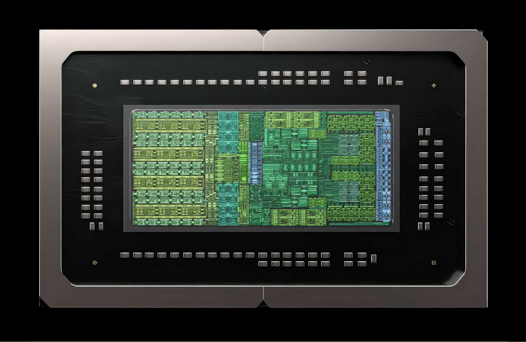
A technical breakdown of the GB10 system-on-chip powering NVIDIA's newly shipped DGX Spark hardware.
Key Takeaways
- NVIDIA co-developed the GB10 SoC with MediaTek, leading to the newly released DGX Spark system.
- The hardware was initially revealed as Project DIGITS at CES in January before its March renaming.
- Chief Architect Andi Skende detailed the system's architecture at the Hot Chips conference in September.
- Unlike separated high-end configurations, the GB10 integrates CPU and GPU dies via a 2.5D multi-die package.
Synthesized Analysis
Subbu reports on the Grace-Blackwell GB10 SoC, the processor powering NVIDIA DGX Spark. Originally announced as Project DIGITS at CES in January, the hardware was renamed before shipping this October. According to Chief Architect Andi Skende, the chip was co-developed alongside MediaTek. Unlike larger configurations, the GB10 utilizes a 2.5D multi-die package. CPU and GPU dies connect via C2C interconnects.
For Builders: Vitraga's Take
Software Systems Implication
vitraga.com ↗Hardware engineers evaluating edge and local cluster deployments should review how the GB10 handles multi-die CPU and GPU integration. Understanding the 2.5D packaging and C2C interconnect constraints will help teams optimize workloads designed for the newly shipped DGX Spark form factor.
Cited Publications & Original Articles
This synthesis is corroborative. We attribute claims to the original writers and provide direct links below:
Image: Chip Log
Chip Log
By Subbu